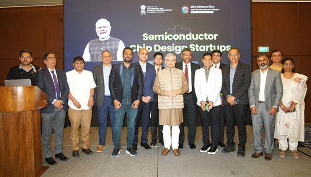
Union Minister for Electronics and Information Technology Ashwini Vaishnaw interacted with semiconductor chip design companies approved under the Design Linked Incentive Scheme of the Semicon India Programme in New Delhi, reaffirming the government’s commitment to building a strong, self-reliant semiconductor design ecosystem in the country.
The interaction focused on reviewing the progress of supported startups, understanding emerging design innovations and outlining the next phase of growth for India’s fabless semiconductor sector. The DLI Scheme is aimed at accelerating domestic chip design capabilities by supporting startups and companies working on system-on-chips, telecom solutions, power management, artificial intelligence and Internet of Things applications.
The companies supported under the scheme are engaged in a wide spectrum of semiconductor design activities, including indigenous SoCs and ASICs for surveillance, networking and embedded systems, RISC-V based processors and accelerators, AI-enabled low-power chips for IoT and edge devices, telecom and wireless chipsets, power management and mixed-signal ICs. Several designs are also targeted at strategic sectors such as automotive, energy, space and defence, strengthening India’s technological self-reliance.
As part of the support framework, advanced electronic design automation tools have been provided, resulting in nearly 2.25 crore tool-hours of usage. Around 67,000 students and more than 1,000 startup engineers are actively engaged. In academic institutions, 122 designs have been taped out, with 56 chips fabricated at the 180 nanometre node at SCL Mohali. Startups have completed 16 tape-outs, leading to six chips fabricated at advanced foundry nodes as small as 12 nanometres. In parallel, 75 patents have been filed by academic institutions and 10 patents by startups.
Addressing the participants, Ashwini Vaishnaw said the government’s ecosystem-driven, multi-year approach to semiconductors is delivering tangible results. He recalled that the programme was conceived in 2022 under the vision of Prime Minister Narendra Modi to build the entire semiconductor value chain, pursue a long-term strategy and transform India into a product-focused nation.
Highlighting the success of the DLI Scheme, the Minister noted that while initial expectations were modest, the programme now supports 24 startups, many of which have completed tape-outs, validated products and gained market traction. He said this validates the government’s approach of removing key barriers faced by semiconductor startups by providing access to advanced tools, IP libraries, wafer and tape-out support.
He underlined that the support extended by the India Semiconductor Mission is globally unique and announced that the government now aims to scale up the programme to enable at least 50 fabless semiconductor companies in the next phase. He expressed confidence that India will see the emergence of globally competitive fabless companies in the coming years.
Referring to recent global engagements, including the World Economic Forum at Davos, the Minister said international industry leaders have increasingly recognised the seriousness, scale and execution capability of India’s semiconductor programme. From early scepticism, global perception has shifted towards strong interest in partnering with India’s growing ecosystem.
The Minister outlined a focused strategy around six key semiconductor design domains: compute systems, RF and wireless, networking, power management, sensors and memory. These domains, he said, form the building blocks of modern electronic systems and are critical for applications across defence, space, automotive, railways and emerging technologies.
On infrastructure, he said SCL Mohali will continue to support tape-outs at the 180 nanometre node, while advanced nodes up to 28 nanometres will be enabled through the upcoming fabrication facility at Dholera. He highlighted sustained efforts in talent development, noting that more than 67,000 semiconductor professionals have already been trained against a ten-year target of 85,000.
Looking ahead, the Minister said that by 2029, India would be capable of designing and manufacturing chips required for nearly 70 to 75 percent of domestic applications. Under Semicon 2.0, the focus will expand to advanced manufacturing, with a roadmap to achieve 3 nanometre and 2 nanometre technology nodes, positioning India among the top global semiconductor nations by 2035.
He further noted that startups supported under the DLI Scheme have attracted nearly ₹430 crore in venture capital funding, with 14 of the 24 startups securing external investment. The India Semiconductor Mission, launched four years ago, has also led to 10 projects under construction, four projects expected to begin production this year and large-scale training across 315 academic institutions.
The Minister announced that the government will institute Deep Tech Awards in 2026 to recognise excellence and innovation in semiconductors, artificial intelligence, biotechnology, space and other deep technology domains. The first edition of the awards is expected to be held later this year.
During the interaction, several startups showcased their tape-out milestones and commercialisation roadmaps enabled through DLI funding and tool support. They emphasised the importance of chip-level indigenisation for trusted supply chains and credited the scheme for enabling their progress. The interaction was attended by Secretary MeitY S Krishnan and CEO India Semiconductor Mission Amitesh Kumar Sinha.